Synthesis, characterization, and design of molecular materials, especially molecular conductors (including superconductors), have been undertaken. Molecular conductors exhibit a variety of physical properties which can be systematically understood on the basis of "simple" and "clear" electronic structures. From a chemical point of view, the most fascinating character of the molecular conductor is its "designability", that is, we can finely control solid state properties with chemical modifications of the molecule. The newly synthesized materials are characterized by the X-ray diffraction method and physical measurements (electrical conductivity...etc.). The electronic structure is investigated by the band structure calculation. All these results are devoted to the design of new molecular materials.
- Magnetic order structure in a triangular lattice of molecular conductor (Cation+)[Pd(dmit)2]2
- Unconventional ground state near the AF-QSL quantum phase transition in Pd(dmit)2 salts
- Hall effect measurements under pressure in β'-X[Pd(dmit)2]2
- Discovery of a single-component molecular superconductor
- Dirac cone formation in a single-component molecular crystal under high pressure
- Electron spin resonance and cyclotron resonance of the bi-layer molecular conductor (Me-3,5-DIP)[Ni(dmit)2]2
- High-density carrier doping into an organic Mott insulator using electric-double-layer transistor
- Criticality at the metal-insulator transition on organic Mott FET
Assign: Ueda, Fujiyama, Cui, Kato; H. Yamamoto
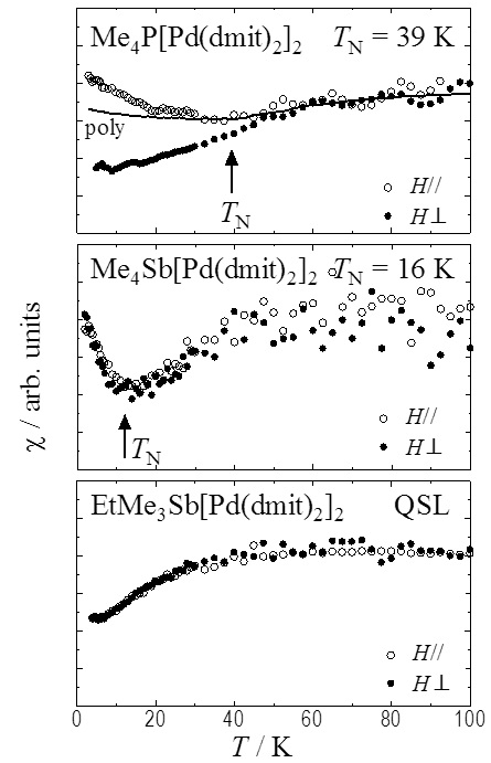
It is proposed that the quantum spin liquid (QSL) is realized in localized spins on a 2D-triangular lattice, many experimental and theoretical studies have done. Almost all of (Cation+)[Pd(dmit)2]2 salts, include EtMe3Sb salt, belong to same structure. In the crystal, spin -1/2 units, [Pd(dmit)2]2-, form 2D isosceles triangular structure, which is characterized by a frustration parameter t'/t; t and t' are interdimer transfer integrals. The frustration parameter can be tuned by changing counter cation. The ground state varies with t'/t; the QSL is realized in the crystal, of which t'/t is nearly 1, and Antiferromagnetic long-range order (AFLO) is realized in the crystal, of which t'/t is small1. To reveal a magnetic structure of the AFLO neighboring the QSL in t'/t -T phase diagram is important for understanding spin behavior in frustrated spin system. So, we studied the magnetic anisotropy of some cation salts down to 2 K by MPMS, relationship between magnetic ordering structure and frustration.
No magnetic anisotropy was observed in the EtMe3Sb salt; a magnetic susceptibility of parallel to 2D lattice was same as one of perpendicular to 2D lattice. No anisotropic magnetic ordering was confirmed. It is consistent to the previous magnetic torque measurement. In most AFLO crystals (Me4P salt ~Et2Me2As salt; 0.62 ≤ t'/t ≤ 0.87), the anisotropic magnetic susceptibility was split to one of perpendicular and parallel to 2D lattice below Neel temperature (TN). The direction of the magnetic easy axis is determined as a perpendicular direction. On the other hand, the ground state of the Me4Sb salt, which is adjacent to QSL on the t'/t-T phase diagram and shows the most low TN (16K), is understood as AFLO; nevertheless no magnetic anisotropy was observed like as the QSL crystal below TN. Another strange behavior was observed on the M-H curves. A spin-flop transition like behaver was observed on AFLO salts except for the Me4Sb salt. No magnetic anomaly was observed in the Me4Sb salt and EtMe3Sb salt up to 7 T. Recently, we succeeded in fine control of t'/t by using mixed-cation salts, which will lead us to reveal boundary behavior around QSL2. It is already reported that the ground state of Et2Me2As1-xSbx[Pd(dmit)2]2 salt was varied from typical AFLO to QSL by adding Et2Me2Sb+ with t'/t tuned. So, the study, which was performed on Et2Me2As1-xSbx[Pd(dmit)2]2 salt, investigate whether the specific feature observed in the Me4Sb salt is a characteristic one for Me4Sb+ or is realized depend on t'/t tune. The 0 ≤ x ≤ 0.05 salts behaved as typical AFLO with the magnetic anisotropy and the spin-flop like behavior. The 0.35 ≤ x salts realized the QSL. On the other hand, the magnetic behavior of 0.15 ≤ x ≤ 0.25 salts were same as one of the Me4Sb salt. It is concluded that the special magnetic state, which has a characteristic intermediate between AFLO and QSL, is caused as a neighboring phase of QSL by geometric frustration of triangular lattice. Its magnetic state is not clear. The 13C NMR measurement are performing to reveal microspic view of the magnetic state of the Me4Sb salt.
Magnetic susceptibility of (Cation+)[Pd(dmit)2]2
References
[1] K. Kanoda and R. Kato, Annu. Rev. Condens. Matter Phys., 2, 167-188 (2011).
[2] R. Kato et al., Phys. Status Solidi B249(5), 999-1003 (2012).
Assign: Fujiyama, Ueda, Kato
An electronic phase diagram of a triangular-lattice molecular conductor system, (Cation) [Pd(dmit)2]2, is proposed as a function of t'/t, the ratio of transfer integrals between dimerized molecules. We focused on the electronic state in the vicinity of quantum phase transition between the classical antiferromagnetism and the quantum spin liquid state. The electronic state of Me4Sb[Pd(dmit)2]2 of which antiferromagnetic transition temperature is as low as T~10K is considered to be located in the critical region. An anomalous absence of the magnetic anisotropy below the transition temperature was suggested by the susceptibility measurements.
The 13C NMR spectra using randomly oriented crystals show a significant broadening below 10 K, showing magnetic transition. However, the spectra in the ordered state has a sharp structure at the K=0 frequency, which suggests a charge disproportionation in this material. So far no charge ordering originating from inter-site Coulomb repulsion is theoretically proposed in the series of material, which is distinct from other molecular conductors such as TMTTF or BEDT-TTF charge transfer salts. The NMR spectra point out an importance of intra-molecular electronic modulation of (Cation) [Pd(dmit)2]2 system.
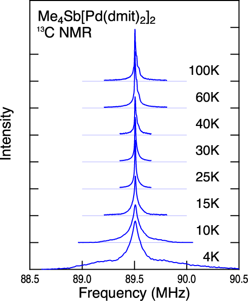
13C NMR spectra of Me4Sb[Pd(dmit)2]2. A magnetic transition is shown below 10K with distinctive charge densities.
Assign: Iwase, Ueda, Cui, Kato; H. Yamamoto
Anion radical salts β'-X[Pd(dmit)2]2 (dmit = 1,3-dithiole-2-thione-4,5-dithiolate, X: closed-shell monovalent cations) shows various electronic states depending on the modulation of the crystal structure. A parameter which characterizes electronic states is an anisotropy of triangles assuming the dimer [Pd(dmit)2]2- as an unit. The ground state changes from the antiferromagnetic state to the charge order state through a quantum spin liquid state with increasing the parameter, t'/t; where t and t' are the transfer integrals between dimers.
The project of this year is to find a new aspect of the electronic property by conducting Hall effect measurement in β'-Et2Me2As[Pd(dmit)2]2. This material shows the antiferromagnetic phase transition at about 16 K at ambient pressure and shows superconductivity under the pressure. We made a new probe for the Hall effect measurement and checked the performance in the first half of the year. A stepping motor module (400 steps) for the rotation of the probe in the magnetic field is attached at the above of the probe. A 1/128 micro-step driver is used to rotate the stepping motor controlled by a PC. The probe rotates smoothly with the step less than 0.001 degree.
The Hall effect and the resistivity measurements are conducted in the single crystals of β'-Et2Me2As[Pd(dmit)2]2 and β'-Et2Me2As0.5Sb0.5[Pd(dmit)2]2. Five- or six-probe measurements with both methods of sample rotation and magnetic field sweeping are used.
1. Hall coefficient RH at 200 K is positive (~10-2 (cm3C-1)), suggesting the main contributions to the conductivity are holes. RH increases with decreasing the temperature. The behavior, however, suppresses with increasing the pressure. One of three samples shows an inversion of the sign of the RH at low temperatures. However, the low temperature behavior is not reproducible.
2. The magnetic field dependence of the magnetoresistance Rxx changes from the positive to negative below about 30 K.
3. The sample dependence in the resistivity of β'-Et2Me2As[Pd(dmit)2]2 is observed. More than ten samples are required to determine the intrinsic resistivity behavior. The superconductivity is clearly observed.
4. In the mix-crystals of As and Sb, the critical pressure of the superconducting transition tends to increase with increasing the As concentration.
5. Some anomalies in the resistivity are observed at low temperatures under pressure (for example 8 kbar, 20 K). The anomalies become weak by the pressure. This behavior may relate to the anomaly in the Hall coefficient. It is interesting that if the effect of the magnetic phase transition or the quantum spin liquid state (paramagnetic) reflects on the transport measurements.
We have revealed some new transport aspects on β'-X[Pd(dmit)2]2 in this year. Additional measurements to acquire reliable data are under way.
Assign: Cui, Iwase, Kato; H. Kobayashi, Ishibashi, Sasa, A. Kobayashi
One of the first lessons in physics at school is that molecular materials are insulators and thus rendering a crystal of one of them electrically conducting has been of major importance. In the early seventies, the idea of partially depopulating the HOMO (highest occupied molecular orbital) or partially populating the LUMO (lowest unoccupied molecular orbital) in planar π-conjugated molecules consisting of chalcogen heterocycles was attempted in the syntheses of charge-transfer salts. This opened the field and not only did metallic conductivity was observed to very low temperatures but superconductivity was ultimately put in evidence; first under pressure and later at ambient pressure. Such materials are not single-component anymore but contain other cations or anions and sometimes solvents (even water). Yet the idea of finding metallic conductivity and superconductivity in neutral molecules did not fade away. The breakthrough came with idea, that has developed through experience, that lengthening the planar molecules with more chalcogen heterocycles and the synthesis of [Ni(tmdt)2] (Ni(S6C9H6)2, tmdt = trimethylenetetrathiafulvalenedithiolate), where on each side of the nickel is three sulfur heterocycles and the trimethylene capping the end. It was the first ambient pressure single-component molecular metal with the Fermi surface that has been characterized experimentally and theoretically.[1] Because the molecular system has soft lattice, an application of high pressure to molecular crystals is a very effective way to discover new single component molecular metals. Recently, in [Ni(ptdt)2] (Ni(S8C9H6)2, ptdt = propylenedithiotetrathiafulvalenedithiolate), a metallic state will be stabilized at ambient pressure. However, this was not case and a metallic state was observed only above 19 GPa. [2] We also successfully observed the metallic state for a wide temperature range above 15.9 GPa in a single-component molecule crystal of [Ni(dmit)2] (Ni(S5C3)2: dmit=1,3-dithiole-2- thione-4,5-dithiolate).[3] Very recently, we have measured the high-pressure electrical resistivity of [Ni(hfdt)2] (hfdt = bis(trifluoromethyl) tetrathiafulvalenedithiolate) up to ü`10 GPa using a diamond anvil cell (DAC), and found the first single-component molecular superconductor.[4]
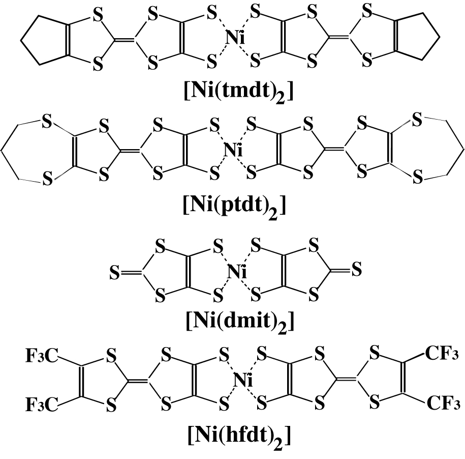
Figure 1: Molecule structures
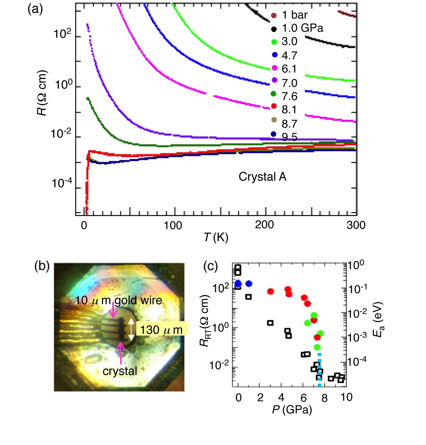
Figure 2: (a) The temperature dependences of the resistivities of [Ni(hfdt)2]. (b) A picture of a sample in a DAC. (c) Pressure dependences of the room-temperature resistivity and the activation energies (Ea).
Black plate crystals of [Ni(hfdt)2] were grown electrochemically, the ambient pressure, the resistivity showed semiconducting behavior with a room-temperature resistivity of ü`6 ü~ 102 āČ cm and an activation energy (Ea) of 0.14 eV (Figure 2a,c). The room-temperature resistivity decreased rapidly with increasing pressure (P) at P < 7 GPa (Figure 2c), but the pressure dependence of Ea was rather sluggish at P < 6 GPa. Around 7.3 GPa, Ea decreased very sharply, and the metallic state appeared above 7.5 GPa. Above 7.3 GPa, the pressure dependence of the room-temperature resistivity became very small (ü`3 ü~ 10?3 āČ cm). As shown in Figure 2a, at 7.6 GPa, the resistivity gradually decreased down to ü`85 K, then increased fairly rapidly with decreasing temperatures, and a very small resistivity decrease was detected around the lowest experimental temperature (ü`3.3 K). A sharp resistivity drop indicating the superconducting transition was observed around 8.1 GPa. The onset temperature of the superconducting transition was ü`5.5 K. This resistivity behavior clearly indicates the existence of a single-component molecular superconductor. Above 8.7 GPa, a superconducting transition was not observed at least above 3.3 K. A slight resistivity increase was observed at low temperatures (8.7 and 9.5 GPa). The magnetic field dependence of the resistivity was measured up to 7 T. As shown in Figure 3a, the resistivity drop was suppressed by applying a magnetic field. Similar measurements were also made for other crystals (crystal B (Figure 3b). A small resistivity drop at 7.6 GPa and the almost complete suppression of this resistivity drop at 7 T indicated that the lowest pressure of the superconducting region in the pressure?temperature (P-T) phase diagram was ü`7.5 GPa. The P?T phase diagram is presented in Figure 3c. The superconducting phase appeared in the pressure range of 7.5-8.6 GPa at T > 3.3 K.
To understand the origin of pressure dependence of the conductivity, we performed first-principle electronic-structure calculations as a function of pressure. Starting from the experimental structure at ambient pressure and 200 K, the lattice parameters and atomic positions are computationally optimized applying a hydrostatic pressure of 6-11 GPa. We used our computational code QMAS (Quantum MAterials Simulator) based on the projector augmented-wave method with the generalized gradient approximation (GGA) to describe exchange-correlation energy. The calculated band gap at ambient pressure (ü`0.12 eV) is significantly smaller than the value expected from the activation energy (Ea) of the resistivity. This is general tendency of the GGA (and the local density approximation also). At 6 GPa, the band gap is calculated to be 0.01 eV, and at 8 GPa, the band gap disappears and the system becomes a semimetal with Fermi surfaces consisting of small hole and electron pockets as shown in Figure 4. This pressure variation of the band gap is consistent with the variation of the activation energy shown in Figure 2c. The sizes of Fermi surfaces grow with pressure. At 10 GPa, there are quasi-2D hole and electron Fermi surfaces as shown in Figure 4c.
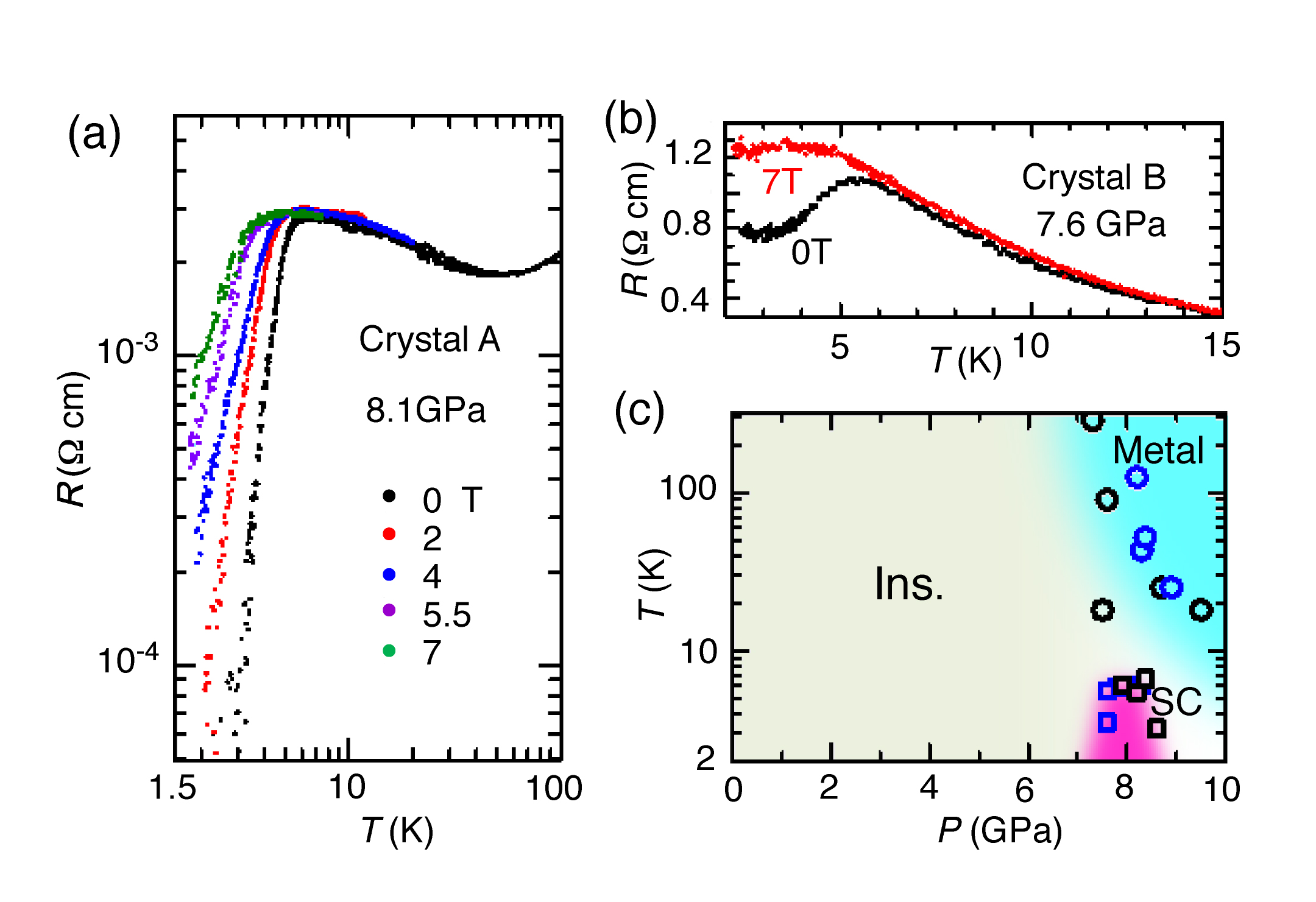
Figure 3: (a) The resistivity behavior under magnetic field. (b) Another example of the magnetic field dependence of resistivity (c) P-T phase diagram.
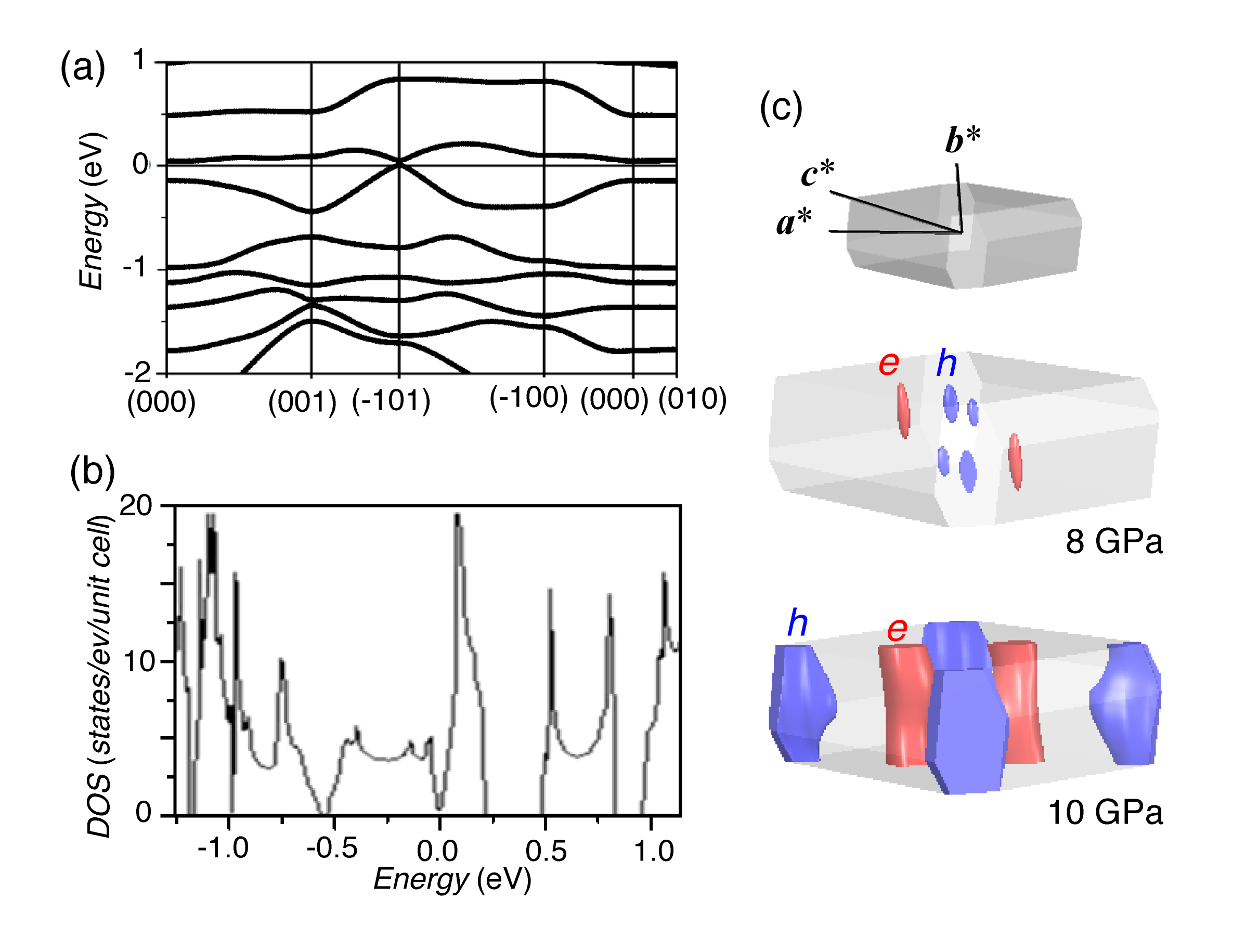
Figure 4: (a) Electronic band energy dispersion at 8 GPa. (b) Electronic density of states at 8 GPa. (c) Electron and hole Fermi surfaces at 8 and 10 GPa
References
[1] Tanaka, H.; Okano, Y.; Kobayashi, H.; Suzuki, W.; Kobayashi, A. Science 2001, 291, 285
[2] Cui, H. B.; Brooks, J. S.; Kobayashi, A.; Kobayashi, H. J. Am. Chem. Soc. 2009, 131, 6358
[3] Cui, H. B.; Tsumuraya, T.; Miyazaki, T.; Y. Okano, Y.; Kato, R. Eur. J. Inorg. Chem. 2014, 24, 3837
[4] Cui H. B.; Kobayashi H.; Ishibashi S.; Sasa M.; Iwase F.; Kato R.; and Kobayashi A. J. Am. Chem. Soc. 2014, 136, 7619
Assign: Tsumuraya, Cui, Kato; Kino, Miyazaki
Dirac cone is an unusual electronic state showing linear dispersion relations with a crossing point near the Fermi level. The existence of Dirac points near the Fermi level is responsible for many important properties of the materials such as high electron mobility and conductivity that originated from the fact that effective electron mass is zero. The notable examples are graphene, the surface state of topological insulators, and molecular conductors [α-(BEDT-TTF)I3 under pressure of 1.5 GPa].
Most single-component molecular crystals show insulating or semiconducting properties at ambient pressure. Among them, a family of metal (M) dithiolene complexes has attracted much attention ever since a metallic state was realized in Ni(tmdt)2 at ambient pressure [1]. The metallic state originates from the relatively small energy difference between the HOMO and LUMO of the constituent molecule (calculated as ~ 0.6 eV) and ā╬-conjugation extended over the ligands. Recently. Even if the systems are insulating at ambient pressure, by application of pressure, such single-component compounds possibly turn into metallic or superconducting states [2]. We recently examined resistivity measurements for various single-component systems up to 25 GPa using diamond anvil cell, and some of them turn into metallic or superconducting state under the pressure above 8 GPa. However, only from experiments, it is difficult to determine the structural and electronic properties under high-pressure. First-principles density functional theory (DFT) calculationü@method can determine such properties of materials independently from experimental results. Therefore, the scheme is useful to understand the mechanisms under such high-pressure condition.
In this study, we perform structural optimizations for various single-component molecular crystals under pressure, and found that anisotropic linear (Dirac cone) dispersions near the Fermi level in Pd(dddt)2 (dddt = 5,6-dihydro-1, 4-dithiin-2, 3-dithiolate) at 8 GPa. Recent electrical resistivity measured at 12.6 GPa indicates temperature independent behavior as is observed in the massless Dirac fermion system, α-(BEDT-TTF)2I3 [3]. Figure 1 shows the crystal structure of Pd(dddt)2 at ambient pressure which has monoclinic lattice with the space group of P21/c. As plotted in Fig. 2 (a), the calculated band structure shows insulating with a finite band gap of 2.1 eV.
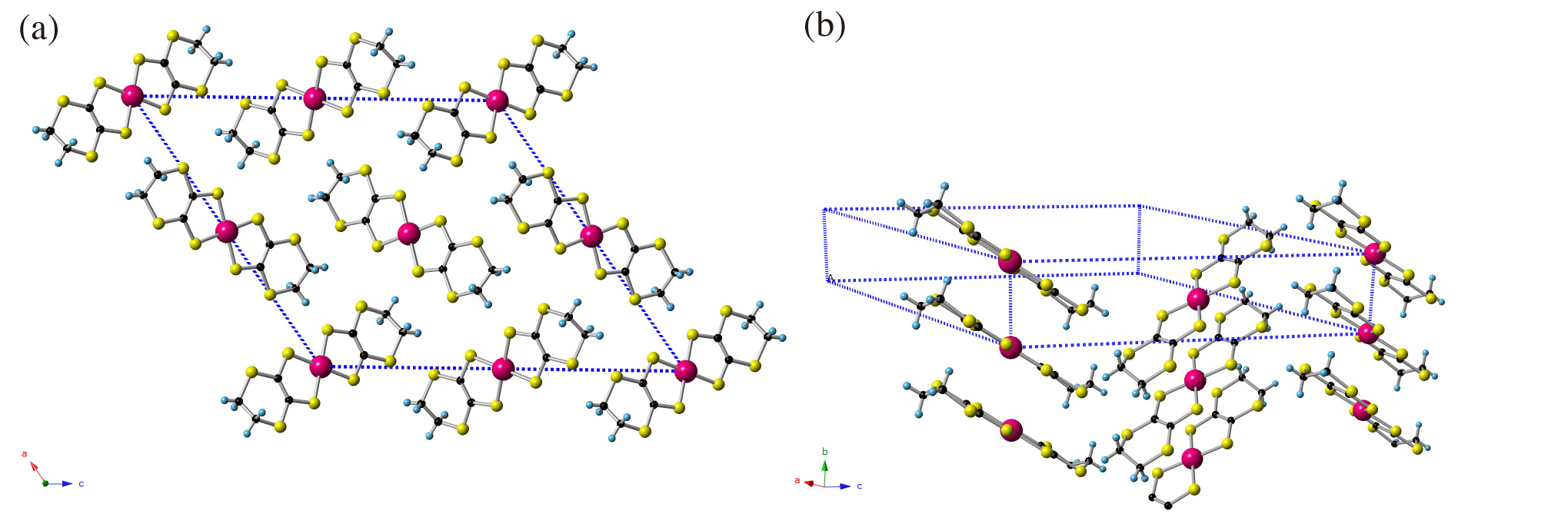
Figure 1: Crystal structure of Pd(dddt)2 at ambient pressure (a) a-c plane (b) b-c plane.
To understand microscopic mechanism of the Dirac cone formation, we analyze the electronic structure under pressure. As we mentioned above, the top of valence bands are mostly composed of the HOMO of Pd(dddt)2 molecule at ambient pressure, the LUMO of neighboring molecule is hybridized to the valence band under the high pressure. The intermolecular hybridization between the frontier molecular orbitals increases due to the reduced intermolecular distances. The multi-orbital nature enhanced by the pressure effect has important role for the Dirac cone formation. Furthermore, we found that the pressure effect changes the dimensionality of the electronic structure; Two-dimensional hypothetical Fermi surfaces were obtained at -0.08/+0.05 eV from the Fermi level. Note that intermolecular overlaps along b and c directions form 2D band structure.
We also performed extended Huckel + tight-binding calculations by taking into account the HOMO-LUMO overlaps. The calculated tight-binding band structure is generally in agreement with the DFT bands. The HOMO-LUMO overlap integral is not negligible even at ambient pressure, and the value of the overlap integrals along b and c axis significantly increase under the pressure of 8 GPa. The fact that one of the two LUMO bands is convex downward where one of the two overlap integrals has a negative sign is important to realize the band crossing near the Fermi level.
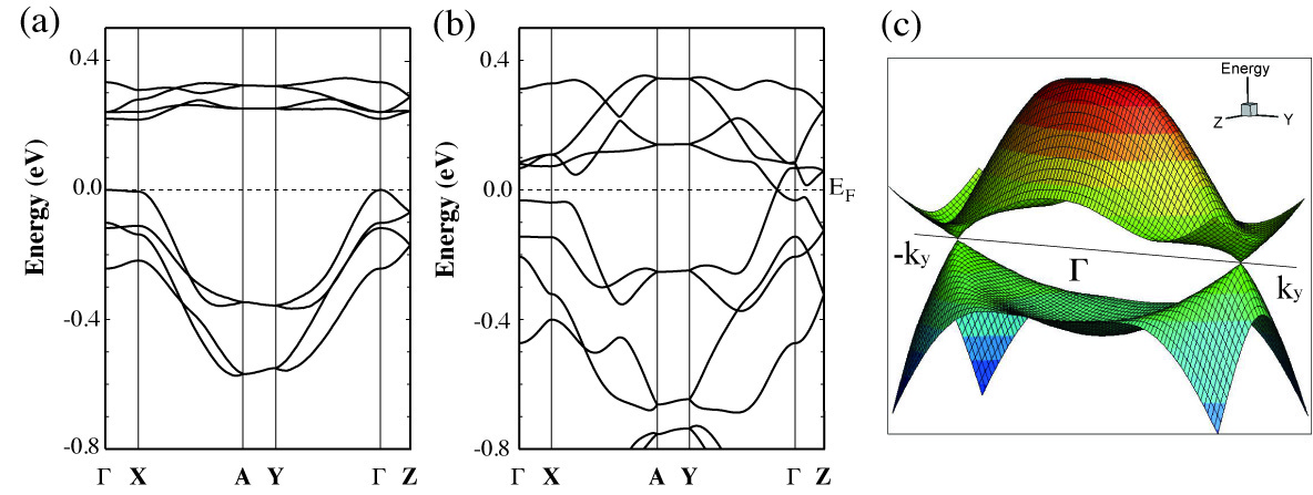
Figure 2: Band structure of Pd(dddt)2. (a) Ambient pressure (b) 8 GPa, and (c) three dimensional band structure along āĪ-Y line.
[1] H. Tanaka, Y. Okano, H. Kobayashi, W. Suzuki, A. Kobayashi, Science, 291, 285 (2001).
[2] H. B. Cui, T. Tsumuraya, T. Miyazaki, Y. Okano, and R. Kato, Eur. J. Inorg. Chem, 24, 3837 (2014).
[3] H. B. Cui, H. Kobayashi, S. Ishibashi, M. Sasa, F. Iwase, R. Kato, and A. Kobayashi, J. Am. Chem. Soc., 136, 7619 (2014).
[4] N. Tajima, S. Sugawara , M. Tamura, Y. Nishio, and K. Kajita, J. Phys. Soc. Jpn. 75, 051010 (2006).
Assign: Oshima, Cui, Kato; Kosaka, Uruichi, H. Yamamoto
Interactions between conducting electrons and itinerant electrons have been a great interest among scientists since such interactions lead to a variety of exotic physical phenomena such as giant magnetoresistance and field-induced superconductivity, and so on. For instance, λ-(BETS)2FeCl4 (BETS = bis(ethylenedithio)tetraselena fulvalene) is one of the molecular conductors where not-negligible interactions between conducting π-electrons and localized 3d electrons exist. [1] The conducting π electrons become insulating due to the antiferromagnetic long-range order of the 3d electrons (Fe3+, S=5/2), and then, the metallic state recovers when the localized spins are completely polarized with a strong magnetic field. If more magnetic field is applied, the metallic state becomes superconducting above 17 T. [1] Therefore, interaction between localized and itinerant electrons leads to an intriguing physical phenomena.
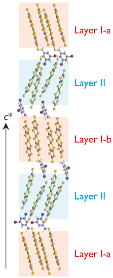
For the past few years, bi-layer type molecular conductors, which fully utilize the design flexibility of molecular complexes and the molecular degree of freedom, have been synthesized. [2-4] One of such kind of bi-layer molecular conductors is (Me-3,5-DIP)[Ni(dmit)2]2 (Me=methyl, DIP=diiodopyridinium, dmit=1,3-dithiole-2-thione-4,5- dithiolate). [2] As shown in Fig. 1, due to the molecular arrangement of Me-3,5-DIP cations, the Ni(dmit)2 layers take two different kinds of layer structure. The Ni(dmit)2 molecules are strongly dimerized in Layer I, and Ni(dmit)2 molecules take a spanning overlap structure in Layer II. It is predicted from the band calculation that Layer I is a Mott insulator and Layer II is metallic with a 2D Fermi surface. Quantum oscillations and NMR measurements results are consistent with this prediction. [5,6] Moreover, the results of the quantum oscillations suggest that the 2D Fermi surface of Layer II (conducting π electrons) is split due to the internal field from Layer I (localized π electrons). [6] This suggests a non-negligible interaction between the itinerant and localized π electrons exists. On the other hand, the magnetism of this material, especially Layer I, is still under debate. NMR predicts an antiferromagnetic long range order of the localized electrons or a strong fluctuation of the spin correlations around 2 K, however, no long range order has been observed from the specific heat measurements. [6] This is why we have focused on the electron spin resonance (ESR) and cyclotron resonance (CR) measurements, which are the most directly and microscopic methods to probe the localized and itinerant electrons. It is possible to know the electronic states of both layers, which have different physical properties, by observing individually the ESR in Layer I and the CR in Layer II.
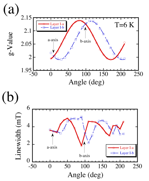
Figure 2 is the ESR results where the magnetic field is rotated within the ab-plane. As shown in Fig. 2(a), a large g-anisotropy is observed which is due to the mixing of the d-orbit in the Ni(dmit)2 molecule. The principal axes of the g-factors are related to the stacking direction and its perpendicular direction of Ni(dmit)2 dimers. Therefore, the origins of the two ESR signals belong to Layer I-a and I-b where the stacking direction is slightly different for each layer. Moreover, the observation of two ESR signals suggests that there is no interaction between Layer I-a and I-b. On the other hand, the ESR linewidth also show an interesting feature (Fig. 2(b)). The angular dependence of linewidth for Layer I-a and I-b are both similar accompanied with an unconventional linewidth narrowing around the b-axis. These anomalies nearby the b-axis might be related to the peculiar magnetoresistance due to the momentum shift of the tunneling conduction.
Figure 3 is the transmission spectra of (Me-3,5-DIP)[Ni(dmit)2]2 using millimeter-waves. The magnetic field is applied along the c*-axis. Thanks to the high frequency, a single ESR line, which is expected for this field orientation, is observed along with a broad absorption that can be attributed to the CR arising from Layer II. The effective mass deduced from the resonance field of CR is m*=0.94me where it is far different with the mass obtained from quantum oscillations. From the Kohn's theorem, such difference can be attributed to the strong correlation between Layer I and II.
 |
 |
|
| Figure 1: Crystal structure of (Me -3,5-DIP)[Ni(dmit)2]2. The stack- ing direction of Ni(dmit)2 dimers slightly differ in Layer I-a and I-b. |
Figure 2: Angular dependence of (a) g-value and (b) linewidth in the ab-plane. |
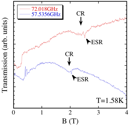
Figure 3: Millimeter-wave measurements for B//c*.
References
[1] S. Uji et al., J. Phys. Soc. Jpn. 75, 051014 (2006).
[2] Y. Kosaka et al., J. Am. Chem. Soc. 129, 3054 (2007)
[3] T. Kusamoto et al., Inorg. Chem. 51, 11645 (2012).
[4] T. Kusamoto et al., Inorg. Chem. 52, 4759 (2013).
[5] S. Fujiyama et al. Phys. Rev. B 77, 060403(R) [6] K. Hazama et al. Phys. Rev. B 83, 165129 (2011).
Assign: Kawasugi, Sato, Kato; Edagawa, Pu, Takenobu, H. Yamamoto
The band theory, which ignores the electron-electron interactions in solids, can predict whether a material is a metal or an insulator. However, a Mott insulator is insulating because of the strong electron-electron interaction although it should be a metal according to the band theory. Since the discovery of high-temperature superconductivity, which emerges in the proximity of the Mott insulating phase, the Mott insulators have been one of the central issues in the condensed matter physics.
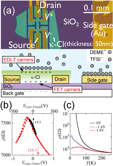
There are two paths from a Mott insulator to a metal or a superconductor. One is to dope charge carriers such as electrons and holes, and the other is to compress the crystal to enhance the band width. To study the Mott transition in organic Mott insulators, the latter method had been usually used because it was suitable to soft materials. Recently, Condensed Molecular Materials Lab succeeded in carrier doping into organic Mott insulators by using the principle of the field-effect transistor (FET) [1]. This method enables parameter control of organic Mott insulators in much wider region of the parameter space and is expected to result in understanding the origin of the superconductivity. However, the doping concentration in the FET was limited up to approximately 10% owing to the withstanding voltage of the gate insulator. In this study, we applied the structure of the electric-double-layer transistor (EDLT), which has attracted much attention as a novel method of high-density carrier doping, to an organic Mott insulator κ-(BEDT-TTF)2Cu[N(CN)2]Cl (abbreviated to κ).
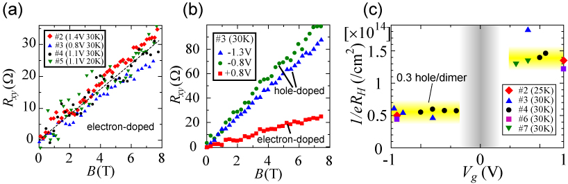
To observe the carrier tunability of the EDLT, we compared the field effect of the EDLT (DEME-TFSI gate) and FET (SiO2 gate) in the same κ-Cl crystal at 220 K. As shown in Fig. 1, the EDLT could induce charge carriers at least four times as much as that of the FET. The electron-doped state became metallic and the hole-doped state also became conducting although it remained an insulator. As a result, we achieved the measurement of the Hall effect both on the electron- and hole-doped state in the same κ-Cl crystal. In a conventional transistor, the carrier density estimated from the Hall coefficient is proportional to the gate voltage. However, on the electron-doped state of this Mott insulator, the carrier density was almost constant against the gate voltage (Fig. 2(a)). The Hall coefficient was approximately 4 /T corresponding to 80~90% of the intrinsic carriers, which should be mobile if the electron-electron interaction was absent. In other words, the gate voltage dependence of the Hall coefficient elucidated that the solidified charge carriers in κ-Cl were melted and became mobile by carrier doping. This is a unique feature of a Mott insulator.
This feature should also be observed on the hole-doped state. The carrier density under hole doping was actually constant against the gate voltage. However, the value was about three times larger than that on the electron-doped side, indicating that the electronic states were distinctly different between the electron- and hole-doped states. Although the exact reason for the small carrier density on the hole-doped side is unclear, it is consistently explained by assuming the pseudogap state which has been predicted in κ-BEDT-TTF salts [2]. Namely, one possible scenario is that the antiferromagnetic spin correlation was suppressed and the Fermi surface recovered on the electron-doped side, while the antiferromagnetic spin correlation survived and the pseudogap state appeared on the hole-doped side. Such an asymmetry of the magnetism has been theoretically predicted so far [3]. In oxide Mott insulators where high-temperature superconductivity emerges, such Hall measurements have not been observed probably because of the complex electronic states. These results represent the essence of the doping asymmetry in a Mott insulator and show the advantage of an organic system as a model material for studying strongly correlated electrons.
(BEDT-TTF = bis(ethylenedithio)tetrathiafulvalene)
References
[1] Kawasugi, Y.; Yamamoto, H. M.; Hosoda, M.; Tajima, N.; Fukunaga, T.; Tsukagoshi, K.; Kato, R. Appl. Phys. Lett. 2008, 92, 243508.
[2] Kang, J.; Yu, S.; Xiang, T.; Li, J. Phys. Rev. B 2011, 84, 064520.
[3] Kyung, B. Phys. Rev. B 2007, 75, 033102.
Assign: Sato, Kawasugi, Kato; Suda, H. Yamamoto
κ-(BEDT-TTF)2[Cu(CN)2]Cl (κ-Cl) is one of the strongly-correlated molecular conductors classified with quasi-two-dimensional Mott insulator, whose electronic feature is governed by strong Coulomb repulsion between carriers at low temperature. Due to the fact that charge injection on Mott insulator can delocalize carriers, we have successfully realized filling-induced Mott transition by manufacturing field-effect transistors (FETs) channeled with single crystal of organic Mott insulators such as κ-Cl and its sister compound κ-Br. Since the electrostatic doping on FETs enables us to finely tune the doping density without introducing any impurities, it is an ideal method to investigate the nature of Mott transition.
In principle, the electronic feature of FET channels should be sensitively affected by properties of the interface between the substrate and molecular-conductor channel. To obtain good interface, we adapt chemically functionalized substrate with self-assembled monolayers (SAMs) terminated by hydrophobic functional group (alkyl C8H17 or perfluoroalkyl C6F13C2H5 groups). In addition, we successfully obtained κ-Cl single crystals with very flat surface whose roughness is under the conduction layer of BEDT-TTF molecules (1.5 nm). As a result, within the range of 20-40 K, the metal-insulator transition (MIT) was induced by high gate voltage V_g (left panel of Fig.2). The conductivity at the transition point is within the Mott-Ioffe-Regel limit: āąü`e2/h (e: unit charge, h: Planck constant), which is a common feature in the MIT of semiconductors with high carrier mobility (e.g. GaAs). In contrast, the Hall effect measurements showed that the observed MIT occurs without change of carrier density (ü`1014 cm-2), which is seemingly unique to the MIT on strongly-correlated materials. The emergence of MIT significantly depends on the condition of κ-Cl/substrate interface, indicating that it is governed by both of disorder and electron correlation (Mott-Anderson transition).
The right panel of Fig.2 depicts a scaling plot of conductivity āą for various Vg, T. According to theory of quantum phase transition, conductivity is given in scaling law in the critical region: āą(T,x)=āąc F(|x-xc | T-1/ā╦z ) due to divergence of correlation length ā╠ and correlation time āč as ā╠üÕ|x-xc |-ā╦ and āčüÕ|x-xc |-zā╦ (ā╦, z: the critical exponents depending on the universality class of transition, x:parameter corresponding to Vg) at the transition. In fact, assuming ā╦z=1.6, all the conductivity points (T=20-35 K) excellently collapse to two curves corresponding to metallic and insulating sides, which tells us that the observed MIT surely satisfies the scaling law. On the other hand, in the lower temperature region (T<10 K), the apparent MIT became absent and logarithmic temperature dependence of transport was uniformly observed as āóāąü`(e2/h) logT for the whole range of measured Vg window. The response to magnetic field, however, alters around the transition point with the inversion of the sign of magnetoresistance. This implies that quantum interference effect as well as electron correlation play important roles at low temperature, and compete with each other depending on the amount of carrier doping. The above result is the first example which provides a detailed feature of the filling-induced Mott-Anderson metal-insulator transition.
(BEDT-TTF = bis(ethylenedithio)tetrathiafulvalene)
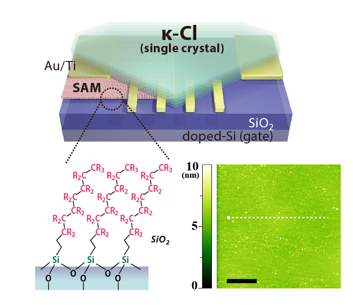
Figure1: Schematic of organic Mott FET with dielec-tric substrate functionalized with SAMüiR = F, Hüj. (Right inset) AFM topography of the surface of thin κ-Cl single crystal. scale bar: 500 nm
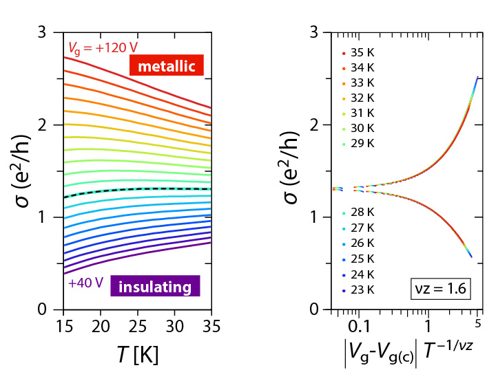
Figure 2: Metal-Insulator transition on κ-Cl/SAM channel induced by electrostatic doping. (Left) Gate-voltage-dependent conductivity as a function of temperature. Separatrix between metallic and insulating state is denoted by broken line. (Right) Scaling plot for conductivity. e2/h=38.7 ā╩S