Condensed Molecular Materials Laboratory pursues possibilities of molecular materials, especially molecular conductors, from the viewpoint of solid state science. The molecular conductors are molecular based electrical conductors including semiconductors, metals, and superconductors. Their components are organic and metal complex molecules (Scheme). The molecular conductors are characterized by
1) Clear and simple electronic structure
2) A variety of physics that originate from low-dimensionality and strongly correlated electrons, etc.
3) Softness
4) Rich chemical design.
Thanks to these characters, the molecular conductor is one of the standard materials in condensed matter and materials physics and interdisciplinary basic science is expanding (Chem. Rev., 104 (2004). Thematic issue for molecular conductors).
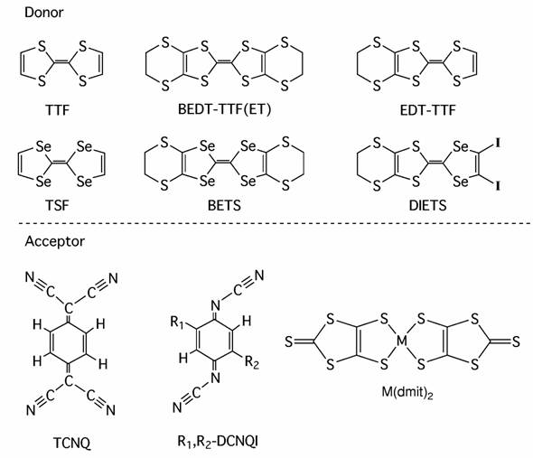
Scheme Components of molecular conductors
Research Topics
- An application of supramolecular chemistry to molecular conductors
(H. M. Yamamoto, Y. Kosaka, A. Nakao, M. Kobayashi, T. Kiss, M. Fujiwara, N. Tajima, and R. Kato)
1.1 Cation radical salts based on TTF (tetrathiafulvalene) derivatives
1.2 Anion radical salts based on M(dmit)2 (dmit=1,3-dithiole-2-thione-4,5-dithiolate; M=Ni, Pd)
- Control of electronic states of molecular conductors with anisotropic strain and extension
(N. Tajima, A. Tajima, J. Eda, T. Yamamoto, T. Imakubo, M. Tamura, and R. Kato)
2.1 Uni-axial strain
2.2 Anisotropic extension
- Development of molecular conductors based on metal-dithiolene complexes
(K. Kubo, A. Nakao, A. Fukaya, Y. Ishii, Y. Shimizu, A. Tajima, N. Tajima, S. Kawamura (Ohira), H. M. Yamamoto, M. Tamura, and R. Kato)
3.1 Systematic studies on a strongly correlated two-dimensional system, Pd(dmit)2 salts
3.2 Development of molecular conductors based on multimetallic dithiolene complexes
- Organic zero-gap-conductor
(N. Tajima, M. Tamura, and R. Kato)
- Photo-induced insulator-metal transition in molecular conductors with the charge ordering state
(N. Tajima and R. Kato)
- Formation of nano-sized crystals of molecular conductors on silicon substrates
(H. M. Yamamoto, H. Ito, T. Suzuki, Y. Kawasugi, M. Ikeda, and R. Kato)
- Development of novel organic semiconductors for organic field effect (OFET) transistors
(M. Ashizawa and R. Kato)
- Theoretical study on conducting organic π systems
(C. Hotta)
- Anisotropy of nonlinear optical responses in organic molecules and semiconductor nanocrystals
(Driven by T. Isoshima, since the period of joining the laboratory in 2001)
9.1 Anisotropy in third-order nonlinear optical responses of organometallic dendrimers
9.2 Ultrafast relaxation of anisotropy in transient absorption of metallophthalocyanine
9.3 Self-organized noncentrosymmetric molecular orientation in vacuum-evaporated organic thin films
- Application of lasers for the development of new technologies
(Driven by T. Kobayashi since the period of joining the laboratory in 1999)
10.1 Production of spin-polarized atoms and electrons
10.2 Simultaneous atomization and ionization of molecules by femtosecond laser ablation
10.3 Production of atomic ions with high kinetic energy
10.4 Femtosecond laser ablation of fullerene (C60) molecule
1. An application of supramolecular chemistry to molecular conductors
(H. M. Yamamoto, Y. Kosaka, A. Nakao, M. Kobayashi, T. Kiss, M. Fujiwara, N. Tajima, and R. Kato)
In the development of novel molecular metals and superconductors since the first organic superconductor was discovered in 1980, construction of higher dimensional electronic structures has been a matter of serious interest in order to suppress the metal-insulator transition. In this process, it has been revealed that electronic states of molecular conductors are quite sensitive to molecular arrangement and orientation which are governed by various intermolecular interactions. Therefore, design of the inter-molecular interaction is indispensable in the rational development of the molecular conductors to still higher forms. An introduction of supramolecular chemistry is a possible solution to this problem. This means that we change our viewpoint from molecules to supramolecular synthons. The supramolecular synthons are spatial arrangements of intermolecular interactions and play the same focusing role in supramolecular synthesis that conventional synthons do in molecular synthesis (G. R. Desiraju, Angew. Chem. Int. Ed. Engl., 34 (1995) 2311). We have developed various molecular conductors containing supramolecular assemblies based on two types of supramolecular synthons, the iodine-based halogen bond and the tellurium-based secondary bond.
Carbon-bound iodine atoms are known to act as Lewis-acids and form short contacts with various species which can act as a Lewis-base (for example, -CN, -Cl, -Br, and =S). These non-covalent interactions that are classified into the halogen bond can be strong and directional enough to control the assembly of molecules in crystal. Tellurium has a strong tendency to form secondary bonds in crystalline compounds. We used the Te…S type non-covalent interaction as a supramolecular synthon in anion radical salts.
1.1 Cation radical salts based on TTF (tetrathiafulvalene) derivatives
We prepared organic metals based on BEDT-TTF (Bis(ethylenedithio) tetrathiafulvalene; ET), where neutral molecules with the -C≡C-I group, DIA (diiodoacetylene), IIB (iodoethynylbenzene) and pBIB (p-bis(iodoethynyl)benzene), form one-dimensional (1D) supramolecular chains with the halide anions (Cl- and Br-) through the halogen bond -I•••X (Fig. 1) [H. M. Yamamoto, et al., J. Mater. Chem., 11, (2001) 1034]. All these salts exhibit the so-called β-type donor arrangement. Notably, negative charges on the chain are diluted with increasing the unit length. Since the donor/anion ratios in these salts are 2/1 for the DIA…Br chain, 5/2 for the IIB…Br chain, and 3/1 for the pBIB…Br chain, the formal charge of the donor molecule is tuned (+0.5→+0.4→+0.33) with the decrease in density of the negative charge on the anion chain (Fig. 1).
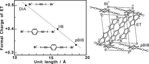
Fig. 1 (left) Crystal structure of (ET)3Br(pBIB). (right) Relation between the formal charge of ET and the unit length of the anionic supramolecular chain in (ET)2Br(DIA), (ET)5Br2(IIB), and (ET)3Br(pBIB).
The above results indicate that the formal charge of ET can be correlated to the unit area within the anion layer. For example, since one ET molecule usually occupies 25-30 Å2 in the conduction layer, the unit area of ca. 90 Å2 / e- is a condition for the unusual formal charge of +1/3. (ET)3X(pBIB) satisfies this condition. In most of the cation radical salts, the formal (averaged) charge of the donor molecule is +1/2. We demonstrated that the formal charge can be tuned with the design of the supramolecular anion layer.
All these salts are metallic down to the lowest temperature. They belong to a typical two-dimensional (2D) electronic system. (ET)2Br(DIA) is recognized as a standard 2D metal system and a variety of physical measurements on quantum oscillations including angle-dependent magnetoresistance oscillation (AMRO), Shubnikov-de Haas (SdH) oscillation, and cyclotron resonance were performed [S. Uji, et al., Phys. Rev. B, 68, (2003) 064420]. Photoemission spectroscopy of (ET)3Br(pBIB) exhibits a Fermi edge which is much clearer than those of other organic conductors. The observed electronic structure near the Fermi energy can be well explained by the first principles band calculation. Angle resolved photoemission spectroscopy was also successfully performed and the band dispersion was observed for the first time as the 2D organic material. For the analog (ET)3Cl(DFBIB) (DFBIB = 1,4-difluoro-2,5-bis(iodoethynyl)benzene), the out-of-plane resistivity in transverse magnetic fields was found to obey a simple formula
 , where ρ⊥(B) is the magnetic field (B)-dependent resistivity and β is a parameter that depends on the material and the temperature [R. Jindo, et al., J. Phys. Soc. Jpn., 75, (2006) 013705]. This is the first example of quasi-2D metals, the magnetoresistance of which is explained by an analytical formula in wide ranges of temperature and magnetic field.
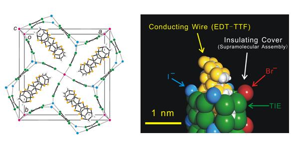
Fig. 2 Crystal structure for (EDT-TTF)4BrI2(TIE)5. The dotted lines denote the halogen bond (left). The nanowire structure is also presented in CPK modeling (right). White, gray, yellow, magenta, green, and sky blue denote hydrogen, carbon, sulfur, bromide ion, iodine, and iodide ion, respectively.
We found that iodine-containing neutral molecules, TIE (tetraiodoethylene), DFBIB, and HFTIEB (1,1',3,3',5,5'-hexafluoro-2,2',4,4'-tris(iodoethynyl)-biphenyl) form anionic supramolecules with halide anions (Cl-, Br-, I-) in cation radical salts based on TTF derivatives. These anion networks with 1D channels accommodate cation radicals of organic donors and form supramolecular insulating networks sheathing conducting nanowires based on organic cation radicals (Fig. 2). The size and shape as well as the orientation (tilt) of the donors are matched by the self-organization of the insulating sheaths in all cases, providing a pea-in-a-pod example in supramolecular chemistry. The results highlight the importance of insulating networks that divide the conducting π-π stacks into independent nanowires. (TSF)Cl(HFTIEB) (TSF = tetraselenafulvalene) with insulating layer of one nanometer thickness exhibits eight orders of magnitude anisotropy in its resistivity, indicating high potential of the supramolecular network as sheathing material. The observation of such networks leads us to propose a roadmap for future development towards multi-dimensional memory devices.
Except for single component molecular conductors, molecular conductors are classified into the ion radical salt where cation and anion govern the electronic state. We emphasize, however, that the neutral molecule can act as the third parameter by means of the supramolecular assembly. It should be noted that the neutral molecules do not require a charge adjustment in designing the supramolecular framework and can accept a variety of functional substituents.
1.2 Anion radical salts based on M(dmit)2 (dmit=1,3-dithiole-2-thione-4,5-dithiolate; M=Ni, Pd)
The metal complex M(dmit)2 has been widely used in conducting or magnetic materials. In conducting anion radical salts of M(dmit)2, the closed-shell counter cations seem to form the "spectator" part that does not contribute to the formation of the conduction band. The crystal of the molecular conductor, however, is a stage where every man must play a part. We introduced the iodine bond and the Te-based secondary bond into the anion radical salts based on M(dmit)2, which make the molecular architecture designable.
We prepared five new Ni(dmit)2 anion radical salts with Te-containing closed-shell cations, Me3Te+ and MOT+ (1-oxa-4-methyl-4-telluracyclohexane). X-ray crystal structure analyses show that all the salts are characterized by short Te…S contacts between the Te-containing cations and the terminal thioketone groups of Ni(dmit)2 (3.41∼3.85 Å) which influence molecular packing of the Ni(dmit)2 units and provide a variety of crystal architecture. Electronic structures deeply depend on these unique molecular arrangements. Among them, Me3Te[Ni(dmit)2]2 and α-(MOT)[Ni(dmit)2]2 show metallic behavior (down to 60 and 160 K, respectively) and the resistivity of β-(MOT)[Ni(dmit)2]2 is almost independent down to 40 K where a moderate upturn is observed [M. Fujiwara, and R. Kato, J. Chem. Soc., Dalton Trans., (2002) 3763].
We also prepared two Pd(dmit)2 anion radical salts, Me3Te[Pd(dmit)2]2 and Et2MeTe[Pd(dmit)2]2, where the Te-based cations prop or staple the Pd(dmit)2 units through short supramolecular Te…S contact and have a great influence on the electronic structure (Fig. 3). Each of them has two different types of Fermi surfaces associated with two crystallographically non-equivalent conduction layers in the unit cell. In both salts, the Mott-insulating state is removed and the systems retain the metallic state down to low temperatures even at ambient pressure [R. Kato, et al., Synth. Met., 120, (2001) 675].
The Te(IV)-based cations have the ability to induce novel arrangements of the M(dmit)2 units through intermolecular Te…S contacts. The above results suggest that control of the arrangement of the M(dmit)2 anion radical is feasible by tuning with variously shaped cations.
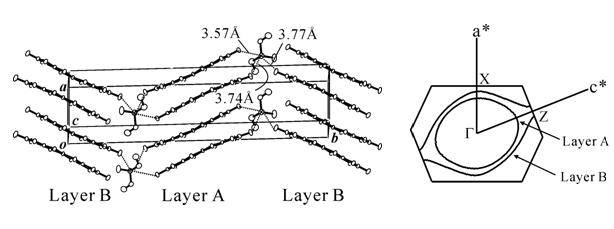
Fig. 3 Crystal structure (left) and calculated Fermi surface (right) for Et2MeTe[Pd(dmit)2]2.
The iodine bond was successfully introduced into the Ni(dmit)2 anion radical salt with use of diiodopyridinium cation, Me-3,5-DIP (N-methyl-3,5-diiodopyridinium), which provided an exotic molecular conductor, (Me-3,5-DIP)[Ni(dmit)2]2. The unit cell has two crystallographically independent anion layers parallel to the ab plane (Fig. 4: Layer I and II). The iodine-containing cations are associated with the terminal thioketone groups of the Ni(dmit)2 anion in both layers through two kinds of short I…S supramolecular interactions, leading to two kinds of Ni(dmit)2 arrangements. In Layer I, Ni(dmit)2 anions show strong dimerization and Layer I is in a Mott insulating state which displays paramagnetism based on a localized spin on the dimer unit [Ni(dmit)2]2-. On the other hand, in Layer II, Ni(dmit)2 anions form a noncolumnar structure that includes a overlapping mode where one molecule overlaps with two molecules, which affords a 2D Fermi surface with elliptical cross-section. This indicates that Layer II exhibits 2D metallic conduction.
Measurements of electrical resistivity and magnetic susceptibility revealed 2D metallic conduction down to 4.2 K and paramagnetism with antiferromagnetic interaction (Fig. 4). These two contrastive features of the electron, localization and itinerary, coexist in the same crystal. Both stem from molecular π-electrons of Ni(dmit)2 contained separately in each layer: "one" kind of molecule playing "two" contrastive roles. This is the first system where conducting and magnetic π-electrons coexist down to 4.2 K. [Y. Kosaka, et al., J. Am. Chem. Soc., 129, (2007) 3054].
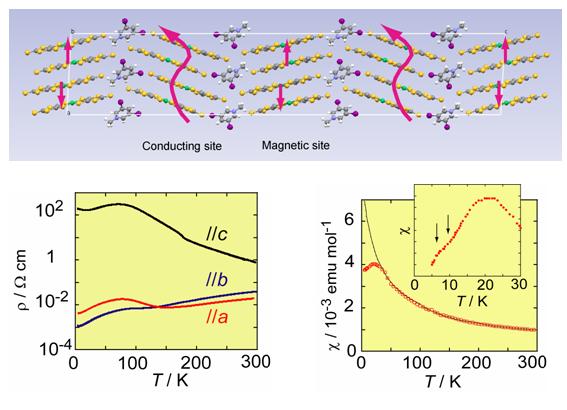
Fig. 4 Crystal structure, anisotropy of resistivity (ρ), and magnetic susceptibility (χ) for (Me-3,5-DIP)[Ni(dmit)2]2.
(N. Tajima, A. Tajima, J. Eda, T. Yamamoto, T. Imakubo, M. Tamura, and R. Kato)
2.1 Uni-axial strain
The electronic states of the molecular conductors can be quite sensitive to the pressure (including chemical pressure) application if they are situated near the phase boundary and are soft enough to allow appreciable changes of molecular arrangement and orientation. The application of hydrostatic pressure has played significant roles in changing the electronic states of low-dimensional molecular conductors. Furthermore, recent development of the uni-axial stress and strain methods has enabled selective or anisotropic regulation of the intermolecular interaction and has provided a powerful means to search for novel electronic states. We examined the uni-axial strain effect and have found unusual electronic states in an organic zero-gap conductor, a supramolecular conductor, a strongly correlated 2D system based on the metal-dmit complex, and an organic charge ordering (CO) system.
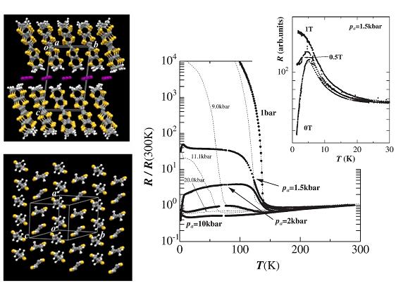
Fig. 5 (left) Crystal structure for α-(ET)2I3. (right) Temperature dependence of the resistance when the sample is strained along the a-axis. The data plotted by broken lines are the resistances under hydrostatic pressure. The upper panel shows the effect of magnetic field on the resistance for the sample under the strain of Pa=1.5 kbar.
An organic conductor α-(ET)2I3 undergoes a metal-insulator transition associated with a charge ordering at ambient pressure (Fig. 5: A zero-gap state and a photo-induced insulator-metal transition for this compound are described in §4 and §5). The uni-axial strain along the a-axis changes the low-temperature electronic state changes from a charge ordered insulating state to a zero-gap conducting state. In between these two states, there appears a superconducting state with Tc = 7 K at 2.5 kbar (Fig. 5). In the zero gap conducting state (Pa=10 kbar in Fig. 5), both the carrier density and mobility change drastically with lowering temperature, leading to temperature-independent resistance. At the lowest temperature, the system is in a high mobility (∼105 cm2/V•s) state. Under the uni-axial strain along the b-axis, on the other hand, this material behaves as a typical quasi-2D metal with large Fermi surface [N. Tajima, et al., J. Phys. Soc. Jpn., 71, (2002) 1832].
Strain-induced superconductivity from an insulating state was found in a supramolecular conductor θ-(DIETS)2[Au(CN)4] (DIETS = Diiodo (ethylenedithio)diselenadithiafulvalene) [T. Imakubo et al., J. Mater. Chem., 12, (2002) 159]. DIETS is an unsymmetrical TTF analogue containing two iodine atoms which can form the iodine bond. The crystal of θ-(DIETS)2[Au(CN)4] contains alternating layers of the donor DIETS and the square planar tetracyanate anion. The donor molecules are arranged in the 'herring bone' fashion. Each iodine atom on the donor molecule is connected to one Au(CN)4 anion through the cyano group and the supramolecular chains are constructed by the iodine bonds (Chain 1 and 2: Fig. 6).
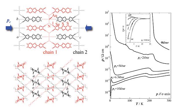
Fig. 6 (left) Crystal structure for θ-(DIETS)2[Au(CN)4]. (right) Temperature dependence of the resistivity under the strain along the c-axis.
Under the ambient pressure, this salt is a semiconductor at high temperatures above 226 K, where a transition to an insulator occurs. This semiconductor-insulator transition is not suppressed by the application of hydrostatic pressure up to 18 kbar. However, things become quite different under uni-axial strains. Rigid supramolecular I…N contacts between the donor (DIETS) and the anion (Au(CN)4) would provide unusual distortion of the crystal lattice under the uni-axial strain. When the strain is applied along the direction perpendicular to the conduction layer (along the c-axis; Pc in Fig. 6), the system undergoes a superconducting transition with Tc =8.6 K at 10 kbar. Under the c-axis strain, the supramolecular chains 1 and 2 formed by the I…N contact would slide into each other along the c-axis. If there were no supramolecular chain, the c-axis strain would only reduce the distance between the conduction layer and the anion without causing significant structural changes within the conduction layer. Band parameter calculations and conductivity anisotoropy measurements suggest that an increase in the band width associated with the strain leads the system to the metallic (and superconducting) states. The effects of strains parallel to the conduction layer, on the other hand, are very small. These behaviors are in striking contrast to those of the conventional θ-type salts without the supramolecular architecture. Notably, in the metallic state, temperature (T) dependence of the Hall coefficient (RH) and the Hall angle (θH) is expressed as RH ∝ T-1 and cotθH ∝ T2. The same relations are reported for the 2D high-Tc cuprates. These results indicate that the application of the uni-axial strain coupled with supramolecular chemistry provides unique electronic states [N. Tajima et al., J. Phys. Soc. Jpn., 72, (2003) 1014].
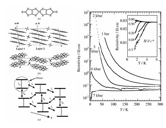
Fig. 7 (left) (a) Molecular structure of Pd(dmit)2, (b) Crystal structure for β'-Me4As[Pd(dmit)2]2. (c) Distorted triangular lattice of Pd(dmit)2 dimers within the conduction layer, where transfer integrals tA, tB, tr, and ts are 448.3, 34.0, 22.7, and 32.4 meV. (right) Temperature dependence of the resistivity (ρ) parallel to the b-axis under the uniaxial strain along the b-axis for the Me4As salt. The inset shows ρ under the magnetic field parallel to the c* direction at 7 kbar.
We demonstrated that the uni-axial strain can effectively control the electronic state of an anion radical salt of Pd(dmit)2, β'-Me4As[Pd(dmit)2]2 (Fig. 7). This compound belongs to a strongly correlated 2D system with a quasi-triangular lattice (Details of a series of Pd(dmit)2 salts are described in §3.1). At low temperature, this system is a Mott insulator under ambient and hydrostatic pressure conditions. When the strain is applied parallel to the b-axis within the a-b conducting layer, the non-metallic behavior is readily suppressed and superconductivity appears at 4 K under 7 kbar. On the other hand, small strain around 2 kbar along both the a- and c*-axis directions enhances the non-metallic behavior. With further increase of the strain, the non-metallic behavior is suppressed, but cannot be removed even at 15 kbar. The b-axis strain reduces the correlation effect by increasing the band width more effectively than the hydrostatic pressure [R. Kato, et al., Phys. Rev. B, 66, (2002) 020508]. The uni-axial strain effect has been used effectively in the systematic study on the electronic states of the Pd(dmit)2 salts (§3.1).
Charge ordering (CO) states in the molecular conductors have attracted intense attention since the inhomogeneous site-charge is often observed for the molecular conductors including highly conducting materials and would be related to the superconducting state. In order to investigate what dictates the CO state, we have examined the CO state of two isostructural cation radical salts, ET5Te2I6 and BETS5Te2I6 (BETS = bis(ethylenedithio) tetraselenafulvalene) using the vibrational spectroscopy. These salts have a non-uniform herringbone structure in the organic layer. Ten donor molecules participate in the conducting layer in a unit cell, wherein the pentamer on the inversion center extends along the stacking direction. We have evidenced the inhomogeneous site-charge distribution not only in the insulating phase but also in the highly conducting state. The site-charges are localized in the low temperature phase. The distribution of the site charge takes the "inner-distribution" in the pentamer, where two charge-rich molecules are located inside the pentamer, for both compounds. The observation of the "inner-distribution" confirms that the inter-site Coulomb interaction mostly contributes to the charge distribution pattern in the CO state. The crystal structures of the present two compounds are almost identical to each other, but the magnitude of the overlap integrals in the BETS salt remarkably differs from that in the ET salt. The high-temperature phase is associated with the frustration between the most stable distribution (inner-distribution) and the secondary stable distribution. The uni-axial strain induces anisotropic contraction of the intermolecular distance. The inter-site Coulomb interaction (and overlap integral) along one direction is then enhanced with almost no enhancement along another direction. Therefore, we examined the dissolution or enhancement of the frustration of the site charge under the uni-axial strain. [T. Yamamoto, et al., Phys. Rev. B, 75, (2007) 205132].
2.2 Anisotropic extension
There were few efforts to apply the negative pressure for the molecular conductors since most of the molecular conductors are fragile. We can expect that the negative pressure induces changes in the structural, electronic and magnetic properties, which would not occur under pressure. As a first step, an instrument for the resistivity measurement under the uni-axial extension has been developed (Fig. 8). The instrument is made from the epoxy resin, which enable us to measure the resistance down to 2 K under the magnetic field without a rupture of the sample. We applied the newly developed instrument to TTF-TCNQ (TCNQ = tetracyanoquinodimethane), θ-(ET)2RbZn(SCN)4 and (DMe-DCNQI-d8)2Cu (DMe-DCNQI = 2,5-dimethyl-dicyanoquinonediimine), which are one-, two- and three-dimensional conductors, respectively. The insulating behavior was enhanced for TTF- TCNQ. The temperature of the resistivity jump was raised for θ-(BEDT-TTF)2RbZn(SCN)4. The insulator-to-metal transition was induced for (DMe-DCNQI-d8)2Cu (Fig. 9) under the anisotropic extension. These phenomena can be explained by the increase (decrease) in the intermolecular distance along the direction parallel (perpendicular) to the anisotropic extension. The anisotropic extension was also applied to β'-(ET)4[H3OGa(C2O4)3]PhNO2, which is an organic superconductor under the ambient pressure. The temperature of the insulator-superconducting transition is raised (5K → 6K) with increasing anisotropic extension parallel to the highly conducting direction (along the b-axis). This is attributed to the increase in the inter-molecular Coulomb repulsion along the perpendicular direction as well as the decrease in the transfer integral along the b direction [T. Yamamoto, et al., Rev. Sci. Instrum., 78 (2007) 083906].
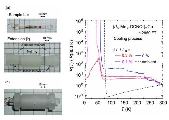
Fig. 8 (left) (a) Sample bar and extension jig, which are made from Stycast 1266. (b) The sample bar installed into the extension jig.
Fig. 9 (right) Temperature dependence of the electrical resistance of (DMe-DCNQI-d8)2Cu under the anisotropic extension along the c-axis (cooling process). The sample bar is made from Stycast 2850FT.
3. Development of molecular conductors based on metal-dithiolene complexes
(K. Kubo, A. Nakao, A. Fukaya, Y. Ishii, Y. Shimizu, A. Tajima, N. Tajima, S. Kawamura (Ohira), H. M. Yamamoto, M. Tamura, and R. Kato)
3.1 Systematic studies on a strongly correlated two-dimensional system, Pd(dmit)2 salts
Metal dithiolene complexes form one of the most important categories of materials as a building block of molecular conductors and magnets with exotic physical properties. Highly conducting anion radical salts of metal dithiolene complexes, including superconductors, have been found [R. Kato, Chem. Rev., 104 (2004) 5319]. Among various types of metal dithiolene complexes which range from electron donors to acceptors, a great interest is given to M(dmit)2 complexes ( M = Ni, Pd, Pt ). Electronic structure and conducting properties of anion radical salts of M(dmit)2 are full of variety depending on the central metal ion, the cation, and external pressure.
A series of 1:2 anion radical salts of the metal dithiolene complex Pd(dmit)2 with the closed-shell cation EtxMe4-xZ+ (Z=N, P, As, Sb; x=0, 1, 2) belongs to a strongly correlated system with a quasi-triangular lattice of [Pd(dmit)2]2 dimers. This system is also characterized by the two-MO (molecular orbital) nature associated with interplay of HOMO and LUMO. All salts have conduction layers, each of which consists of strongly dimerized Pd(dmit)2 units forming a quasi-triangular lattice. The Pd(dmit)2 conduction layer is sandwiched by insulating cation layers. Due to the strong dimerization and small HOMO-LUMO energy difference, the HOMO LUMO band inversion occurs and the narrow and half-filled conduction band is associated with HOMO of the Pd(dmit)2 molecule (Fig. 10).
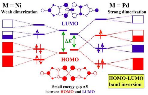
Fig. 10 Schematic electronic structures of M(dmit)2 (M=Ni, Pd) molecule, dimer, and layer.
At ambient pressure, they are Mott insulators with one electron on each dimer and most of them show magnetically frustrated behaviors which is well explained by the model of the spin-1/2 Heisenberg triangular antiferromagnet [M. Tamura and R. Kato, J. Phys.: Condens. Matter, 14, (2002) L729, see also here.]. It is the first time that a molecular material is identified as this basic frustrated antiferromagnetic model by finite temperature behavior. This indicates that frustration is operating in this system. At low temperatures, the spin frustration can be removed by various transitions, including antiferromagnetic ordering, charge ordering (Cation = Et2Me2Sb: 2 Dimer- → Dimer0 + Dimer2- ), and valence bond ordering (Cation = EtMe3P: monoclinic phase), which depends on the cation (Fig. 11). In the charge ordering in the Et2Me2Sb salt, the formation of the HOMO-LUMO double bond plays a significant role to stabilize the neutral dimer, which suggests a new paradigm of the HOMO-LUMO interplay [M. Tamura, et al., Chem. Phys. Lett., 411, (2005) 133]. The valence bond ordering in the EtMe3P salt (monoclinic phase) is similar to the spin-Peierls transition in a quasi-1D case. It is the first case that this kind of phase transition is observed in a 2D spin system [M. Tamura, et al., J. Phys. Soc. Jpn., 75, (2006) 093701].
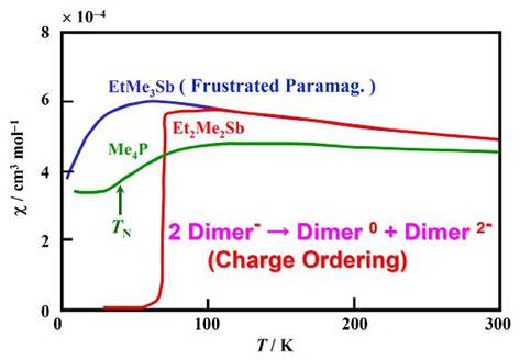
Fig. 11 Temperatue depencece of magnetic susceptibility for (Cation)[Pd(dmit)2]2.
The Mott insulating state of the Pd(dmit)2 salts can be suppressed by the application of hydrostatic or uni-axial pressure. In the case of the Me4P and Me4As salts with higher Néel temperatures (TN > 35 K), the application of hydrostatic pressure cannot suppress the non-metallic behavior. For the Me4As salt, however, the uni-axial pressure (strain) effectively induces the superconductivity (§2.1). The Me4Sb, Et2Me2Z (Z=P, As), and EtMe3As salts with TN = 16∼23 K at ambient pressure, turn metallic and show superconductivity under hydrostatic pressure. The EtMe3Sb salt, which retains the frustrated paramagnetism down to 1.37 K at ambient pressure, also shows a metallic behavior under hydrostatic pressure, but no superconductivity is observed up to 15 kbar. The charge ordering transition in the Et2Me2Sb salt is accompanied by a sharp increase of the resistivity at ambient pressure. The application of hydrostatic pressure turns this resistivity anomaly to a metal-insulator transition. The valence bond ordering state of the EtMe3P salt (monoclinic phase) is situated in the vicinity of the superconducting phase under pressure (Fig. 12) [R. Kato, et al., J. Am. Chem. Soc., 128, (2006) 10016].
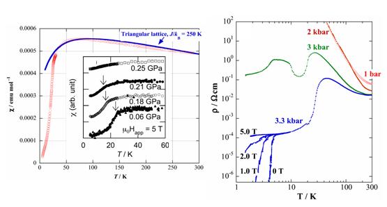
Fig. 12 Magnetic susceptibility (left) and resistivity (right) under hydrostatic pressure for EtMe3P[Pd(dmit)2]2 (monoclinic phase).
The electronic structure of the Pd(dmit)2 salts can be described by the dimer model. In this model, the unit cell contains only one dimer [Pd(dmit)2]2 (Fig. 7c). The interdimer transfer integrals (tB, tr, and ts) determine the dispersion of the conduction band and the intradimer transfer integral tA is approximately correlated to effective on-site Coulomb energy on the dimer Ueff. [M. Tamura and R. Kato, J. Phys. Soc. Jpn., 73, (2004) 3108]. The band width (W) is determined mainly by two larger interdimer transfer integrals tB and ts, and the smallest transfer integral tr governs anisotropy of the band structure.
Crystal structure analysis for β'-Et2Me2P[Pd(dmit)2]2 (Tc = 4 K at 7 kbar) under hydrostatic pressure indicates that the correlation parameter represented by the ratio tA/W decreases steadily with increasing pressure [J.-I. Yamaura, et al., J. Phys. Soc. Jpn., 73, (2004) 976]. This indicates that the insulator-metal transition under the hydrostatic pressure is the Mott transition due to the reduced electron correlation. It should be added that anisotropy of the electronic structure t'/t, where t = tB ≈ ts and t'= tr, is enhanced with increasing pressure. This means an enhancement of the deviation from the regular triangular lattice under pressure, which is consistent with an increase of the Néel temperature under pressure. The cation dependence observed in the pressure effect indicates that in addition to the electron correlation there is another important factor which governs the electronic state of the β'-type Pd(dmit)2 salts (Cation = EtxMe4-xZ+, where Z= P, As, Sb for x=0, 2 and Z=As, Sb for x=1). The tA/W value corresponding to the correlation parameter increases with the cation in the order, Me4P < Me4As < EtMe3As < Et2Me2P ≈ Me4Sb ≈ Et2Me2As < EtMe3Sb < Et2Me2Sb for the room temperature structures. The ease of stabilizing the metallic state with the hydrostatic pressure, however, varies in the same order, except for the Et2Me2Sb salt which undergoes the charge ordering transition. Since the metallic state under the hydrostatic pressure is due to the reduction of the tA/W value, this looks paradoxical. An important clue is that the t'/t value at ambient pressure varies with the cation in the reversed order. This order is related to the deviation from the regular triangular lattice, which suggests an important role of the spin frustration.
The frustration can suppress the long-range spin ordering in the insulating phase. Theoretical studies of ground states in strongly correlated molecular conductors including the system with approximately triangular lattice structure have been systematically performed. It is suggested that the metallic phase appears in the region with weaker electron correlation and stronger frustration. In order to explain the cation dependence observed in the hydrostatic pressure effect, we propose a general picture of the present system, using two parameters, tA/W and t'/t. The former corresponds to the electron correlation parameter and the latter expresses the frustration parameter. Figure 13 shows a very schematic phase diagram for the present system based on the room temperature structures. The hydrostatic pressure effect on the Et2Me2P salt is indicated by arrows which illustrate that the application of pressure decreases both tA/W and t'/t. Simulation of the b-axis strain effect on interdimer transfer integrals and band width for β'-Me4As[Pd(dmit)2]2 based on a simple distortion model suggests that the b-axis strain effectively enhances the inderdimer transfer integral ts, which results in an enhancement of W (Fig. 13). Considering that the b-axis strain hardly affects the intradimer transfer integral tA, we can ascribe an essential role of the b-axis strain in the Me4As salt to more effective reduction of the electron correlation than the hydrostatic pressure.
The Pd(dmit)2 system is a unique playground of the strong correlation physics. The electronic state of this system is governed by the on-site Coulomb energy, the band width, and the degree of frustration, each of which is sensitive to the intra- and interdimer interactions. These parameters can be controlled by chemical and physical methods.
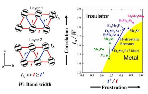
Fig. 13 Schematic phase diagram for β'-(Cation)[Pd(dmit)2]2 based on the room temperature structures.
3.2 Development of molecular conductors based on multimetallic dithiolene complexes
Multimetallic complexes are attracting wide interest as singlemolecule magnets, nanosize self-assembling cages, efficient catalysts, nanowire precursors, and chemical sensors. Few multimetallic dithiolene complexes, however, are known. From the viewpoint of development of novel conducting materials, a versatile method for preparation of the multimetallic dithiolene complexes is of great importance.
Polymetallic nickel complexes bridged by tto (tetrathiooxalate) ligands were successfully prepared by the simple reaction of monometallic nickel complexes [Ni(S-S)2]- (S-S = dithiolene ligand; edo2- = 5,6-dihydro-1,4-dioxine-2,3-dithiolate, dddt2- = 5,6-dihydro-1,4- dithine-2,3-dithiolate) and (Et4N)2(tto) in acetonitrile or DMF (Fig. 14) [K. Kubo, et al., J. Am. Chem. Soc., 128, (2006) 12358]. It was found that this reaction provides trimetallic complexes with two tto bridging ligands as well as bimetallic complexes. Formation of the trimetallic unit in the solution was identified by electrospray ionization (ESI) mass spectrometry (Fig. 14). An HPLC equipped with an ODP (octadecyl polymer) column can be used for purification of these complexes. The trimetallic unitü@[(tto)2Ni3(dddt)2]2- is almost planar except for the terminal ethylene groups (Fig. 15). These new trimetallic complexes are good candidates for single-component molecular metals: the calculated HOMO-LUMO gap of [(tto)2Ni3(dddt)2] is very small (0.15 eV).
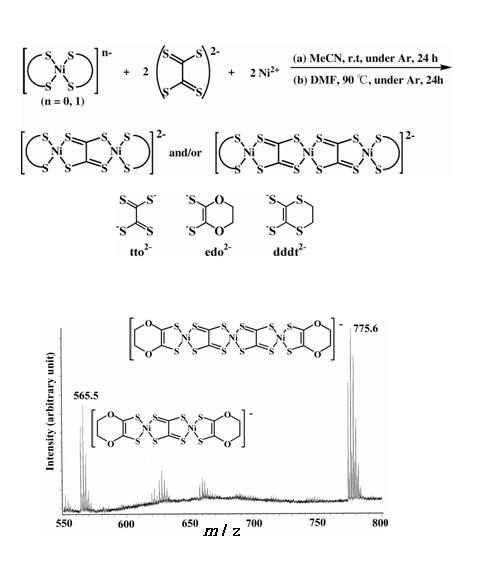
Fig. 14 Synthetic route and ESI-mass spectra for tto-bridged multimetallic dithiolene complexes.
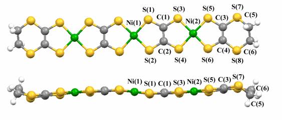
Fig.15 Molecular structure of trimetallic complex [(tto)2Ni3(dddt)2]2-.
4. Organic zero-gap-conductor
(N. Tajima, M. Tamura, and R. Kato)
Massless Dirac Fermions have been found in the organic conductor α-(ET)2I3 (Fig. 5) under high hydrostatic pressure. This is the first 2D zero-gap state discovered in bulk crystals with the layered structure. Electrical conductivity and Hall coefficient of this material under 18 kbar were investigated down to 100 mK. The conductivity is nearly constant from 300 K to 2 K. Measured values of the sheet resistance per conducting ET layer are close to quantum resistance h/e2=25.8 kΩ within a factor of 3, which is almost independent of impurity. In the same temperature region, on the other hand, both carrier density and mobility change by about 6 orders of magnitude, in a manner so that the effects just cancel out giving rise to a quantum resistance h/e2 per layer (Fig. 16). At the lowest temperature, the mobility is as high as 106 cm2/V.s. Another significant point is that the temperature (T) dependence of carrier density (n) obeys not the exponential law but the power law. It obeys n∝T2 from 10 K to 50 K. This result strongly suggests that the system is a zero-gap conductor with 2D Dirac cone type energy dispersion near the Fermi level (Fig. 16). In contrast to graphene, the Dirac cone in this system is highly anisotropic. The present system, therefore, provides a new type of massless Dirac fermions with anisotropic Fermi velocity. Below 10 K, the carrier density is proportional to T3, which indicates that the system is a 3D zero-gap conductor. At the lowest temperature, the carrier density in each conduction layer is as low as 108 / cm2, which is difficult to tune in graphene. However, the carriers are not localized in such a low density state, which is another character of carriers on the Dirac cones.
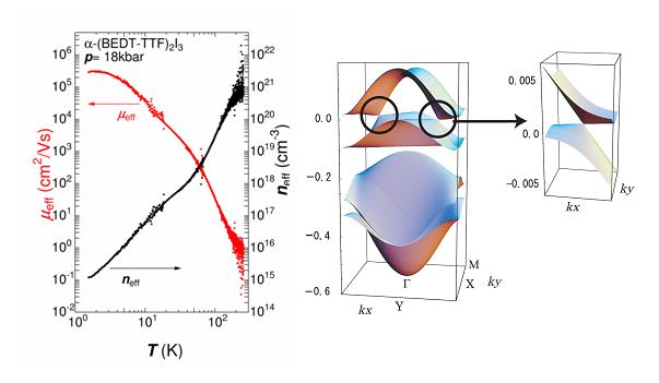
Fig. 16 Mobility (μeff), carrier density (neff) (left), and Dirac cones (right) for α-(ET)2I3
5. Photo-induced insulator-metal transition in molecular conductors with the charge ordering state
(N. Tajima and R. Kato)
A large number of molecular conductors belong to strongly correlated electron systems. The strongly correlated electron systems often exhibit insulating states associated with the self-organization of electrons. Melting of these self-organized electrons can provide drastic phenomena including gigantic responses to external fields. The organic conductor α-(ET)2I3 (Fig. 5) shows a charge ordering state characterized by the self-organization of electrons with a stripe pattern (parallel to the b axis) below 135 K. This charge ordering is driven by inter-site electrostatic repulsions and brings about an insulating state. We have found that the pulsed laser excitation polarized along the stripe induces a persistently conducting state when the pulsed voltage higher than the threshold value is applied (Fig 17). This photo-induced transition can be repeated many times and enables switching accompanied by a drastic resistivity change more than 7 orders of magnitude [N. Tajima, et al., J. Phys. Soc. Jpn., 74, (2005) 511].
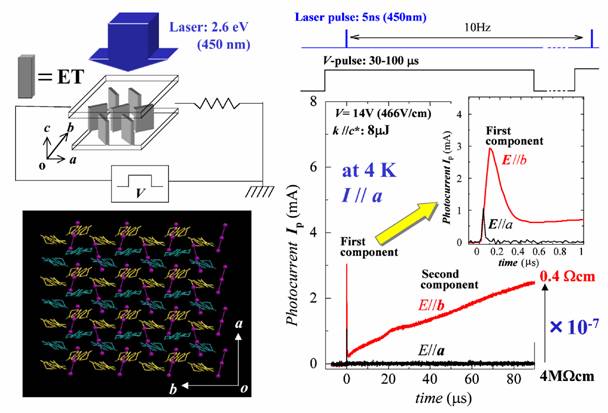
Fig. 17 Stripe pattern and photo-induced insulator-metal transition for α-(ET)2I3.
6. Formation of nano-sized crystals of molecular conductors on silicon substrates
(H. M. Yamamoto, H. Ito, T. Suzuki, Y. Kawasugi, M. Ikeda, and R. Kato)
Although molecular conductors exhibit wide variety of conduction properties comparable to inorganic or polymer-based conductors, their application to micro electric devices is still limited. One of the reasons is a lack of techniques for processing these soft materials in crystalline form. Because the crystals of the molecular conductors are usually insoluble in solvents and nonvolatile due to their ionicity, the fabrication techniques commonly used for organic field effect transistors such as spin-coat or evaporation are inapplicable. In addition, they are too soft to be processed by methods such as sputtering, etching, or milling. Nevertheless, the cleanness of the electron system as well as the functionality of the molecular conductors gives significant motivation for their utilization in many situations including mesoscopic devices. Not only quantum phenomena in these materials, but also size effects upon various phase transitions are interesting. In order to investigate such physical properties of the molecular conductors modified by the size and/or gate voltage, we have developed a new method to grow single crystals on SiO2/Si substrates with the electrochemical crystallization or the chemical reaction between an electrode metal and an organic acceptor [H. M. Yamamoto, et al., J. Am. Chem. Soc., 128, (2006) 700].
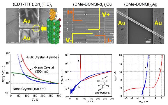
The difference in transition behavior exhibited by nanosized and bulk crystals can be observed. The nano-crystal of supramolecular nanowire (EDT-TTF)4BrI2(TIE)5 (§1.1) retained its conductivity down to 4 K, while the bulk crystal shows high resistance at low temperatures (Fig. 18 left). Four-probe measurements for (DMe-DCNQI-d7)2Cu, which exhibits a sharp metal-insulator transition, were performed using a circuit fabricated on a single crystal (Fig. 18 center). The nano-crystal exhibited a monotonic decrease in resistance down to the lowest temperature, without the expected jump at ca. 80 K, indicating that this crystal retains its metallic character through the present temperature range. It is notable that the contact resistances in these measurements were very low, despite the small contact area (about 1 kΩ for 0.1 μm2 contact area). (DMe-DCNQI)2Ag microcrystal showed rectifying behavior after irradiating half of the crystal (Fig. 18 right). This is considered a consequence of the fact that the irradiation of (DMe-DCNQI)2Ag transforms the crystal from n-type to p-type, and a p-n junction is formed in the single crystal.
Our wet processes for the fabrication of conductive molecular materials on silicon are easy, fast, convenient, and low-cost, and would enable the carrier doping of molecular conductors with the electric field.
7. Development of novel organic semiconductors for organic field effect (OFET) transistors
(M. Ashizawa and R. Kato)
An organic OFET, showing mobility 10-2 cm2/Vs and on/off ratio 104, which are as high as those of dry-processed OFETs of oligothiophenes, has been built by simple drop cast using a solution of a newly synthesized quaterthiophenes-based liquid crystalline compound. X-ray diffraction patterns of the thin film indicate well-defined molecular layers which would originate from their liquid crystalline orders [M. Ashizawa, et al., Chem. Lett., 36, (2007) 708]. The solution process dramatically decrease device fabrication time in comparison with vacuum deposition, and is suitable for industrial application. It should be noted that the present device was fabricated by simple drop-casting and annealing under normal atmospheric conditions.
8. Theoretical study on conducting organic π systems
(C. Hotta)
Quasi-2D organic conductors based on ET type donor molecules are notable for their numbers and variety compared with other electronic systems, which, however, hindered the simple understanding of their nature. There are several categories of materials which are designated as α, β, θ, κ and λ. In each of these polytypes, the transfer integrals are aligned in its own symmetry and it had been quite difficult to relate them with each other. We proposed a new minimal model of quasi-2D organic conductors that could relate many different polytypes for the first time. The polytypes are first classified into two groups; β and θ-types with two independent molecules in the unit cell and α, κ and λ-types with four. After adopting the dimer approximation to the latter group, both could be expressed in an anisotropic triangular lattice model including two sites in the unit cell. Here, the lattice site is regarded as a molecule and a dimer, respectively. Then the difference between the two groups is imposed to the filling of electrons, 3/4 and 1/2, respectively. We provide a way of mapping different polytypes into our minimal model, where a choice of four different band parameters enables the simple relationships among them. The generalized ground state phase diagram of this model on the plane of these band parameters is obtained from the mean-field calculations with on-site and inter-site Coulomb interactions. By associating the actual materials with the results of calculations, their ground state differences are systematically understood [C. Hotta, J. Phys. Soc. Jpn., 72, (2003) 840].
9. Anisotropy of nonlinear optical responses in organic molecules and semiconductor nanocrystals
(Driven by T. Isoshima, since the period of joining the laboratory in 2001)
Microscopic molecular symmetry and macroscopic molecular orientation affect nonlinear optical responses and their anisotropy. Molecular orientation is also affected by the molecular symmetry. Highly symmetric molecules and nanocrystals can possess twofold or threefold degenerate optical transitions, resulting into significantly different anisotropy of nonlinear optical responses. Less symmetric molecules with nondegenerate transitions can also present various anisotropy depending on relative direction of the contributing transitions.
9.1 Anisotropy in third-order nonlinear optical responses of organometallic dendrimers
Dendritic molecules, in which 1D Ru-complex units are linked by π-conjugation, have been investigated by polarization-dependent electroabsorption spectroscopy. The polarization ratio was close to 3, the value for 1D system, suggesting localization of the excited state in each Ru-complex unit, rather than delocalization through π-conjugation (Fig. 19). Colloidal nanocrystals of CdSe were also investigated and the anisotropy suggested two-dimensionality.
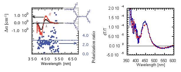
Fig. 19(left) Polarization-dependent 2nd-order electroabsorption spectra and their ratio of Ru-complex dendrimer (inset).
Fig. 20(right) 1st-order electroabsorption spectra of vacuum-evaporated Alq3 thin films. Full line: evaporated under light irradiation. Broken line: evaporated in dark.
9.2 Ultrafast relaxation of anisotropy in transient absorption of metallophthalocyanine
Subpicosecond all-optical switching in resonant wavelengths was examined: use of depolarization due to quick (∼ ps) electronic decoherence of the degenerate excited states can overcome slow (∼ ns) excited-state lifetime of the material. A metallophthalocyanine derivative with fourfold symmetry and twofold degenerate transitions was used as the material. Excited-state lifetime was obtained by subpicosecond pump-probe transient absorption measurement and time-resolved fluorescence measurement, and it was a few nanosecond. Optical Kerr-gate configuration was used to demonstrate all-optical switching, and the switching time was as short as 500 fs, nearly four orders of magnitude smaller than the excited-state lifetime.
9.3 Self-organized noncentrosymmetric molecular orientation in vacuum-evaporated organic thin films
Vacuum-deposited tris(8-hydroxyquinolinato) aluminum(III) (Alq3) thin films show spontaneous buildup of giant surface potential (GSP) as high as 28 V at 560 nm thickness, when deposited in dark. Irradiation of visible light reduces GSP, but the mechanism was not understood yet. By first-order electroabsorption spectroscopy, we revealed that noncentrosymmetric molecular orientation exists before and after GSP reduction, and that the order parameter of molecular orientation is similar to that obtained from magnitude of GSP. These results indicate that GSP reduction is due to electrostatic screening by photogenerated carrier, rather than photoinduced randomization of molecular orientation. Dependence on film deposition method was also investigated, and it was found that vacuum-evaporated films present noncentrosymmetric molecular orientation and that films deposited by wet methods (spin coating or casting method) do not present noncentrosymmetry, suggesting that the vacuum evaporation process plays a dominant roll for formation of noncentrosymmetric molecular orientation (Fig. 20) .
10. Application of lasers for the development of new technologies
(Driven by T. Kobayashi since the period of joining the laboratory in 1999)
10.1 Production of spin-polarized atoms and electrons
Conventional technique for the production of a spin-polarized electron is the photo-ionization of a GaAs based thin layer with a circular-polarized laser beam. However, thin layer can be easily damaged by the ionization laser. As for the production of a spin-polarized ion, some experimental techniques such as optical-pumping method are proposed but they are not yet practical for use.
We have developed two-color excitation scheme for the production of a spin-polarized electron and a spin-polarized atomic ion, simultaneously. In our experiment, strontium atom [Sr (1S0)] is excited to the ionic state [Sr+ (2S1/2)] through the 3P1 state both with a linear-polarized and a circular-polarized laser beams. We have obtained spin-polarization ratio as high as 70%. This value is dependent on the character of the ionic state and we are searching for the ionic state to obtain higher polarization ratio. [T. Nakajima, et al., Appl. Phys. Lett., 83, (2003) 2103, N. Yonekura, et al., J. Chem. Phys., 120, (2004) 1806].
10.2 Simultaneous atomization and ionization of molecules by femtosecond laser ablation
For the development of highly quantitative technique for the genome expression profile analysis, we have applied the femtosecond simultaneous atomization and ionization (fs-SAI) method to detect label ions in the sample. This technique is simple and versatile but found to be less sensitive for the detection of extremely rare genome expression. We have estimated the detection efficiency of our system by measuring number of ions from well-calibrated sample and found it to be only 10-3 of the calculated value. In order to improve the sensitivity, we tried to find out the reason for such low detection efficiency. By capturing the time development of ablation plasma with a gated CCD camera, we found only a few percents of ions in the plasma could be accelerated by an external electric field. In order to overcome this Debye-shielding, we have designed new electrodes for effective acceleration. [M. Kurata-Nishimura, et al., Appl. Surf. Sci., 197-198, (2002) 715].
10.3 Production of atomic ions with high kinetic energy
We have applied laser ablation for the production and the detection of atoms and ions in solid samples. Femtosecond laser ablation (fsLA) is unique as compared with conventional nanosecond laser ablation (nsLA) because fsLA produces atoms and ions with high kinetic energies (K.E.). In the case of Samarium ion, for example, we found K.E. amounted as large as 250 eV corresponding to that of 80 photons of ablation laser. High K.E. can be attributed to the Coulomb explosion mechanism in the case of fsLA although thermal evaporation works in the case of nsLA. We found that the once ablated surface produces atoms and ions with only low K.E. at the second or later ablation because the surface is changed into amorphous phase. (Fig. 21) [T. Kobayashi, et al., J. Phys. Conf., 59, (2007) 364].
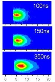
Fig. 21 Longitudinal axis [mm]
10.4 Femtosecond laser ablation of fullerene (C60) molecule
By femtosecond laser ablation (fsLA), molecules are easily dissociated into atomic ions. Ionization and fragmentation of solid C60 dispersed on a silicon plate are investigated by fsLA. Bimodal mass distribution with large fragment ions C60-2n+ (0≤n≤11) and small fragment ions Cn+ (13≤n≤28), formation of dimer ion (C60)2+, and delayed ionization of C60 have been observed. Metastable dissociation of small fragment ions Cn+ has been observed for the first time, which suggests different structures of fragment ions compared with those of well-studied carbon cluster ions. From these observations, strong coupling of laser energy to electronic degrees of freedom of solid C60 has been revealed for fsLA as compared with excitation in the gas phase. (Fig. 22) [T. Kobayashi, et al., J. Chem. Phys., 126, (2007) 061101].
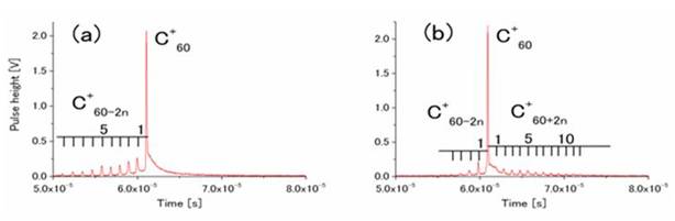
Fig. 22 Product ion species by femtosecond laser ablation with (a) λ=400nm and (b) λ=800 nm.